What We Do Begins with Why You're Doing It
At AMFitzgerald, we believe big-picture strategy is the first step to successful microtechnology innovation.
That's why we always want to understand the Why, and specify the What, before we start work. This is especially important when you consider that developing new technology and products is a very time-consuming and expensive process. Most MEMS and photonic products have needed millions of dollars and years to achieve full commercialization.
What does this mean?
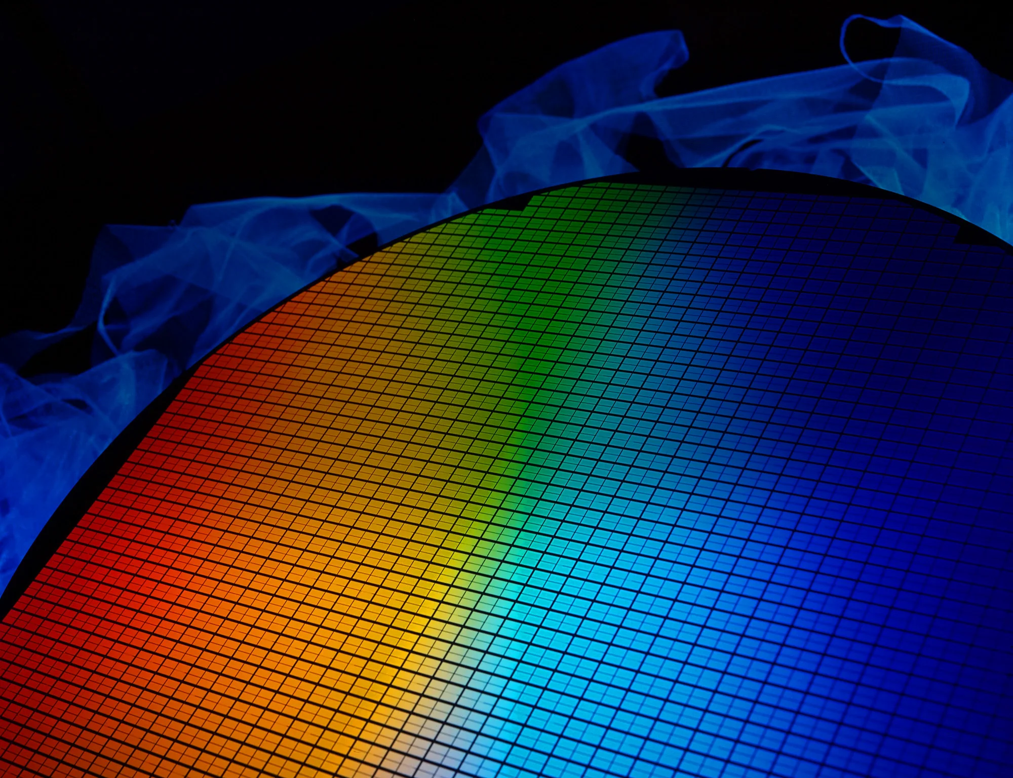
We develop devices with volume wafer manufacturing in mind.
We consider system integration and testing requirements from the very beginning.
We believe simulation and design verification are essential to successful development and manufacturing.
We use a progressive evolution of wafer-based prototypes to successfully develop complex products. Starting with simple prototypes, we increase the complexity over the series before finally achieving full function.
We ensure each development phase consists of sequenced tasks designed to discover, address, and eliminate the technical and business risks of complex product development.
And keep in mind . . .
As the customer, you own all the IP we develop. This simple model enables you to plan manufacturing scale-up with confidence and certainty.
The AMFitzgerald Innovation Process
“AMFitzgerald worked with us to develop a custom MEMS die from start to finish, fabricated the first prototypes, and concluded with selection of a commercial manufacturer. AMFitzgerald was an integrated member of our team and contributed greatly to our success.”