September 2020: Planet-Scale Processing of Silicates


Ancient CMP: cross-section of basalt columns, polished flat by a glacier. Note the fine lines that were created by grit trapped in the moving glacier.
In the eastern Sierra Nevada mountains, near Mammoth Lakes, California, is a geological phenomenon: a cliffside lined with thousands of 10-20 meter tall pillars of basalt. The organized rock columns are so incongruous with the surrounding high altitude pine forest that they seem supernatural. Shepherds who frequented the area in the 1800’s named it the “Devil’s Woodpile.” Today, it’s a popular park called the Devils Postpile National Monument.
To a MEMS engineer, this odd rock cliff bears a striking resemblance to the columnar grains in thin film PZT or ZnO. What a mind bender to see familiar shapes from SEM images towering overhead.
Like PZT or ZnO, a special set of environmental conditions created the Devils Postpile. It was not, however, the result of grain growth; instead, the Postpile formed from a pool of lava which then cracked into a network of polygons as it cooled. (More like misprocessed thick photoresist!).
On top of the Devils Postpile, one particular area has a smooth surface which reveals the cross-sections of the polygonal columns, 50-100 cm in width. This most unusual stone patio was formed by the water, pressure, and motion of a passing Ice Age glacier, a massive-scale version of chemical mechanical polishing (CMP). Basalt rock is primarily composed of SiO2 (45-52% by weight) and other metal oxides, such as TiO2, Al2O3 and MgO; all familiar MEMS materials, just in a much larger format.
Four kilometers from the Postpile is the stunning 30 meter tall Rainbow Falls, etched through two layers of volcanic rock. The top masking layer of rock is harder than the thick underlayer of softer rhyodacite. Water pouring over the edge erodes the soft rock at a faster rate, leaving a re-entrant cliff face and thereby creating a beautiful waterfall.
An idle thought while hiking on a hot summer day: Is geology just a planet-scale version of MEMS processes?
June 2020: When nanotechnology meets chocolate
In the third month of work from home in California due to the COVID-19 pandemic, many companies may be starting to wonder, what’s the point of having an office anymore?
Here’s one delicious reason why: a coffee break chat among researchers at ETH Zürich led to discovery of a method for making chocolate brilliantly colorful using nanotechnology, instead of dye. It’s not unexpected that this happy event occurred in Switzerland, a country having centuries-old traditions in both chocolate-making and precision engineering.


Structural color in chocolates made at ETH Zurich and in the feathers of a Rüppell’s starling (Photo: Ethan Kinsey)
Iridescence is a natural phenomenon, appearing for example in the feathers of birds, wings of butterflies, oyster shells and carapaces of beetles. These creatures make nanoscale patterns in surfaces of chitin, a derivative of glucose, in the form of lines, plates, or holes. The patterns refract light of a comparably-sized wavelength, giving these surfaces colors such as brilliant blue or orange. Due to wave interference, different colors may also appear depending on the surface viewing angle, creating a visual shimmer. Some creatures, such as squids, can even rapidly change their color by controlling the nanoscale spacing of protein layers in their skin through electric charge.
Although the secret of making iridescent chocolate has not yet been revealed by ETH Zürich, we can make a good guess at how they did it: by using e-beam lithography to etch hundred nanometer or so lines on a glass or silicon wafer, and then using that wafer to imprint the pattern onto the surface of a piece of chocolate. In other words, they have made the world’s first nanotechnology chocolate mold.
For those of us who create and research, we really do miss our offices and those random bumps into a colleague, in the hallway or in the breakroom, that could spark an interesting new idea. In the meantime, we look forward to eating iridescent Swiss chocolates for inspiration!
March 2020: MEMS in the fight against COVID-19
On Saturday, 21 March, the USA FDA gave emergency authorization to Cepheid, a California company, to sell a new test for rapid detection of the SARS-CoV-2 virus, which causes COVID-19. Cepheid, founded by Kurt Petersen, M. Allen Northrup and five others in 1996, has been well known in the MEMS community for commercializing microfluidic chip-based polymerase chain reaction (PCR) analysis machines. This is not the first time Cepheid has responded quickly to a biological threat; after the 2001 terrorist attacks in the USA, Cepheid was the first to provide rapid anthrax detection capabilities to the US Postal Service, and still does today.
At the heart of all COVID-19 test protocols (see the WHO protocol and US CDC protocol) is the reverse transcription polymerase chain reaction (RT-PCR) analysis technique. In a very simplified description, PCR uses thermal cycling to amplify the DNA present in a patient’s swab sample, and then using fluorescence optical detection, searches for virus’s specific DNA. The test requires knowing the virus’s genome in the first place; the crucial work to sequence the full genome of SARS-CoV-2 was first published by Chinese scientists for public use on 10 January 2020.
Traditional PCR machines take many hours to thermal cycle and reach a result. MEMS-scale heaters and reaction chambers have a tiny thermal mass, thereby creating a significantly faster heat-cool cycle and enabling a rapid result in minutes.

The first MEMS silicon PCR chip, developed by Northrup et. al. at Lawrence Livermore National Laboratory and licensed to Cepheid (left) and the Cepheid test cartridge today (right) (Source: Northrup MA, Ching MT, White RM, Watson RT, “DNA amplification in a microfabricated reaction chamber,” Transducers 1993, Yokohama, Japan. pp. 924–926.)
Research on MEMS-based PCR systems has continued steadily since the early 1990s. Today, researchers have been focusing on developing highly-integrated, lower cost systems specifically for point of care use. One example of recent research: a team at Korea’s ETRI and Genesystem have developed a prototype low-cost, handheld PCR system having a polyimide chamber and microheater and an integrated CMOS detector for optical readout of results (figure below).

Cross-section schematic of the chamber, heating module and integrated optical detector in a portable PCR prototype (left) and integrated test cartridge (right). (Source: DS Lee, OR Choi, and YJ Seo, “A Handheld and Battery-Powered Realtime Microfluidic PCR Amplification Device,” Transducers 2019, Berlin, Germany pp. 1063-1065.)
Korea’s quick recruitment of its biotech companies and creation of novel drive-thru testing sites helped it to successfully pinpoint its COVID-19 outbreak and to implement control measures. Let’s hope the Cepheid test can be similarly Effective.
Based on successive epidemics of SARS, MERS, and now COVID-19, rapid PCR test machines, enabled by MEMS technology, are becoming essential medical tools in the fight against viral outbreaks. As continued development lowers their cost, we may hopefully soon have a PCR machine in every doctor’s office.
Please note: AMFitzgerald’s business operations are continuing during the California “shelter in place” order, via remote work.
Update 17 March 2020: Business continues, thanks to our preparations
As a California company, AMFitzgerald has a business continuity plan in place for dealing with natural disasters. When we formulated that plan, we were thinking of risks specific to California, like earthquakes and forest fires, that could disrupt our business for weeks. Now we are facing an unusual event: a “shelter in place” order from our local government through 7 April 2020 to help prevent the spread of COVID-19.
During this period, AMFitzgerald will continue most of its operations, while still complying with local regulations.
We are already operating under our existing business continuity plan, which includes:
All of our employees will be working from home and our IT system is configured to securely support remote work.
Our team is cross-trained and all project duties are documented, so that if someone were to get sick, a colleague will take over their duties.
Meetings among ourselves and with our clients will occur solely by Zoom video web conference, as is already our normal business practice for working with remote clients. • Fabrication work is suspended for the meantime.
We are monitoring the CDC.gov website and local alerts daily to track the situation and will respond appropriately to evolving conditions.
As a MEMS product development company, we have a well-practiced set of skills for handling engineering unknowns and for navigating novel situations, which regularly occur in our daily business. We’re finding that our skills are also serving us well in this unprecedented event. We anticipate, plan ahead and prepare as best we can; continually gather and analyze new data; preserve optionality when possible; choose actions thoughtfully; and most importantly, keep calm and carry on. Please don’t hesitate to contact us for updates, advice, or just to hear a friendly voice!
February 2020: The evolving MEMS micro-mirror
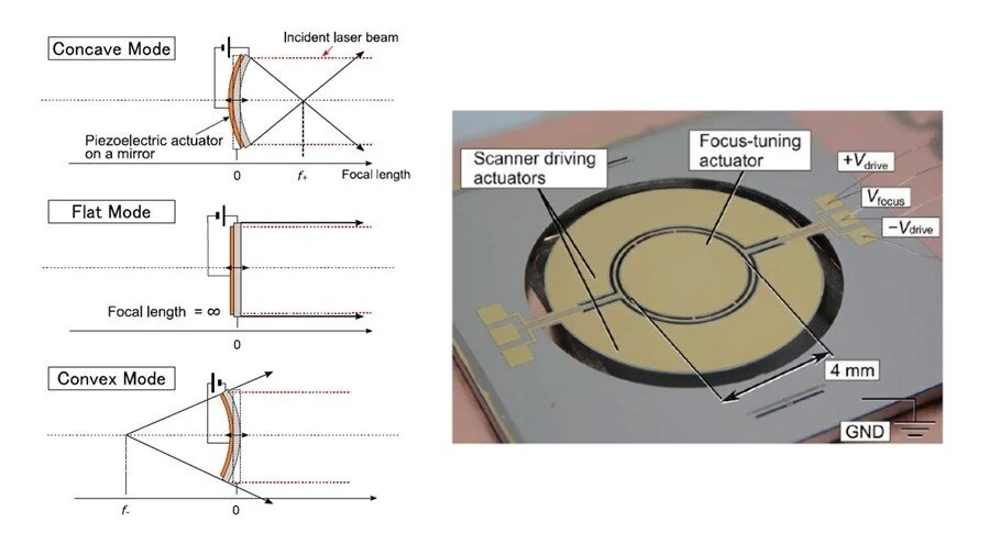
In-plane piezoelectric actuation changes mirror focal length from -120 to +140 mm, enabling 3D beam steering. (Source: S. Inagaki, Y. Okamoto, A. Higo and Y. Mita “High-resolution piezoelectric MEMS scanner fully integrated with focus-tuning and driving actuators,” Transducers 2019.)
Engineers have been developing micro-mirrors since the dawn of MEMS. A tiny, highly reflective platform that can precisely reflect and steer light is eternally useful for optical applications.
Beginning in the 1970s, nearly all MEMS micro-mirrors were actuated electrostatically, using alternating voltages to steer mirrors suspended from slender hinges. (A few others were electromagnetically actuated, for example, by embedding permanent magnets in packaging surrounding the chip.) Early micro-mirror products using electrostatic drive architecture were the Texas Instruments DLP®, countless fiber optic switches, pico-projectors, and even deformable mirror arrays. The arrival of deep reactive ion etching (DRIE) in the 1990s enhanced micro-mirror performance with high-aspect ratio electrostatic comb drives that could drive mirrors with more force and to higher deflection angles.
A new era is now emerging in micro-mirror design. The widespread availability of piezoelectric thin film process technology (PZT, AlN, etc.) is now evolving MEMS micro-mirror designs to new performance levels and abilities. With piezoelectric actuation, higher deflection angles are possible at higher resonant frequencies and lower voltages; significantly, the piezoelectric may be also used to dynamically change the shape of the mirror itself in real time.
In one example of the exciting possibilities of piezoelectric actuation, University of Tokyo researchers have created a mirror having 3-axis beam steering but only two axes of torsional actuation. A piezoelectric film underlying the mirror surface morphs its shape from concave, to flat, to convex, enabling a wide range of focal lengths, and effectively, a third axis of actuation.
Piezoelectric thin film devices also offer many other advantages, such as: they need fewer mask levels and are simpler to fabricate than electrostatic comb drives; they avoid the geometric tolerance issues which plague high aspect ratio DRIE and cause chip to chip performance variations; and they don’t suffer from common electrostatic actuation reliability issues such as snap-in and stiction.
For all these reasons, we anticipate that MEMS devices will continue to evolve away from electrostatic comb drives and towards piezoelectric thin film actuation in the coming decade. Demanding optical applications such as autonomous vehicle LiDAR systems will continue to push MEMS micro-mirror design to achieve exciting new performance levels.
January 2020: Emerging MEMS and Sensor Technologies to Watch in the New Decade

Having a crystal ball would make things so much easier
As a development company whose clients span many technologies and markets, we are frequently asked, “What’s going to be the next big thing in MEMS and sensors?” Unfortunately, we don't possess a crystal ball to accurately predict the future. We do know from history, however, that most of today's blockbuster MEMS technologies originated from academic research. To identify important future technology trends, we attend conferences and read the academic literature. No black magic required, only time and lots of coffee.
We analyzed over 650 papers presented at the 2019 Transducers-Eurosensors Conference, a prestigious international academic conference in MEMS and sensors, in order to identify noteworthy technologies and new devices currently at Technology Readiness Levels 1-4. Our criteria for selection were: commercial relevance, offers a solution to a known or anticipated problem, and technology game changers.
We believe the 2020s will be the decade for:
Commercialization of many piezoelectric-based MEMS sensors, ultimately replacing the older generation MEMS electrostatic comb drive
Widespread use of event-driven or zero-power sensors in IoT applications
Emergence of 2D- and 3D-printed sensors on paper and plastic
For more insights, download our presentation on emerging technology in the 2020s, recently given at the SEMI MSIG Executive Congress. Or read Anne-Françoise Pelé's EETimes feature article about our presentation.
And while we’re going big on predictions, we believe that The Internet of Disposable Things Will Be Made of Paper and Plastic Sensors (IEEE Spectrum). Look for widespread mass production to occur in the 2030s.
Prior Newsletters: 2019 | 2018 I 2017 | 2016 and Older